粉体行业在线展览
粉体行业在线展览


直接联系
German First-Nano System 德国韦氏纳米


法国
面议
1725
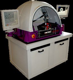
DBT1000 | DBT-1200 | ||||
Speci? cations: Die size: from 300x300μm Thickness: from 3 mil and up 2 basic con? gurations: ? Modul I : XYZ and Theta for Chip handling ? Modul II : XYZ, hi resolution, for multi chuck Shuttle and pin Test centering Z motion with adjustable angle Pickup Tool offset to Crosshair: programmable Test Pin to crosshair: programmable Joystick: proportionnal speed Chip hold on chuck by vacuum Two LCD display, used for wafer handling and for Test Monitoring. Video Target generator for alignment. Lights: Direct and pen LED lights. | Speci?cations: Die size: from 250x250μm (10mil) Thickness: from 75μm, (3 mil) and up 2 basic con? gurations: ? Modul I : XYZ and Theta for Chip handling, ? Modul II : XYZ, hi resolution, for multi chuck Shuttle and pin Test centering Z motion with adjustable angle Pickup Tool offset to Crosshair: programmable Test Pin to crosshair: programmable Joystick: proportionnal speed Chip hold on chuck by vacuum Two LCD display, used for wafer handling and for Test Monitoring. Video Target generator for alignment. Lights: Direct and pen LED lights. Facilities: Power: 100-240vac | ||||
热丝CVD金刚石膜沉积设备HF450
XRD-晶向定位

CVD 真空化学气相沉积设备
等离子体增强化学气相沉积系统CVD
FT-391
BTF-1200C-RTP-CVD
FM-W-PDS
Gasboard-2060
自动划片机
等离子化学气相沉积系统-PECVD